Recent advancements in materials science have led to a breakthrough understanding of boron nanostructures. Researchers at the University of California, Berkeley, have developed a unified design principle that explains how boron can form a diverse range of nanostructures, from fullerenes to two-dimensional sheets. This finding, announced on March 15, 2024, could have significant implications for the development of new materials in various industries.
Boron, positioned next to carbon on the periodic table, exhibits unique bonding capabilities. Unlike carbon, which typically bonds with two or three neighboring atoms, boron can share electrons among multiple atoms, resulting in intricate bond networks. This characteristic allows boron to create various nanostructures, each with distinct properties and potential applications.
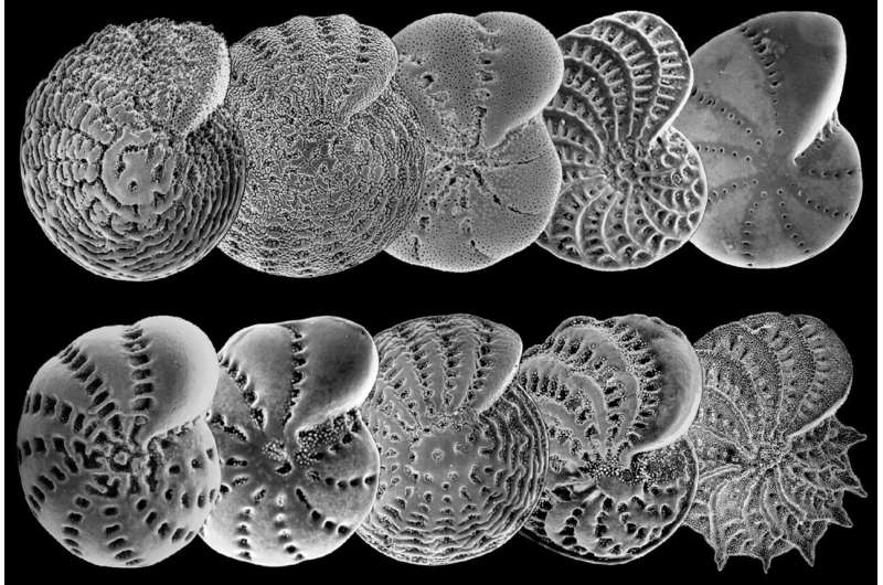
The research highlights two notable forms of boron nanostructures: **boron fullerenes** and **borophenes**. Boron fullerenes are hollow, cage-like molecules that can encapsulate other atoms or molecules, potentially enhancing their functionality. On the other hand, borophenes are ultra-thin metallic sheets formed by boron atoms arranged in triangular and hexagonal patterns. These structures are of particular interest due to their exceptional electrical and thermal conductivity.
Understanding the design principles behind these structures is crucial for harnessing their properties in practical applications. The research team employed advanced computational models to simulate how boron atoms interact and bond under various conditions. This approach allowed them to predict the formation of new nanostructures and optimize their properties for specific uses.
Dr. Maria Johnson, a lead researcher on the project, emphasized the importance of this work. “Our findings provide a framework for designing boron-based materials with tailored properties,” she stated. “This could open doors to innovations in electronics, energy storage, and even drug delivery systems.”
The implications of this research extend beyond academic interest. Industries focused on electronics and materials science could benefit from the unique characteristics of boron nanostructures. For instance, the high electrical conductivity of borophenes makes them promising candidates for next-generation semiconductors. Additionally, boron’s lightweight nature could lead to the development of stronger and lighter materials for aerospace applications.
As researchers continue to explore the potential of boron nanostructures, this unified design principle serves as a foundational step. By elucidating the underlying mechanisms that govern boron’s bonding behavior, scientists can systematically create materials tailored for specific applications.
The discovery of these design principles marks a significant advancement in materials science. Researchers anticipate that by leveraging boron’s unique properties, they can contribute to technological advancements that enhance everyday life. As this field progresses, the versatility of boron may position it as a critical element in future innovations across multiple sectors.
In conclusion, the new understanding of boron nanostructures could revolutionize how materials are designed and utilized, making it an exciting time for researchers and industries alike.